


As our digital footprint grows to support everyday financial transaction through UPI to everyday education of children, electronics touches all walks of Indian society. Electronics is a top import for India [1, 2] – essential to sustain its growth.
Electronics is powered by miniaturization. Every two years a transistor shrinks by half – reducing its footprint to cram double the performance on the same chip. People expect to buy double the RAM or memory in their phones without the phone doubling in size – unable to fit into pockets.
This miniaturization is driven by nanoelectronics innovation. Our national contribution to global nanoelectronics innovation is a key metric of our success in science and technology.
Innovation-driven high-volume semiconductor manufacturing that powers international leaders economically & technologically like USA, Taiwan, Korea and China has eluded India. It is a general feeling that India had missed the “semiconductor bus” in the 1980s by not taking adequate initiatives and making enough investments at the right time. Therefore, the government of India began efforts to harness the potentialities that nanotechnology can provide for revamping the electronics manufacturing industry sector early in the millennium [4]. Ministry of Electronics and Information Technology (MeitY) (then Department of Electronics and Information Technology, DeITY) had started the Nanotechnology Development Programme (NDP) in 2004 to create infrastructure and promote basic research in the areas of nanoelectronics and nanometrology in India [5]. Till then there was no laboratory for fabricating silicon devices in India, even those with 100-micron features.
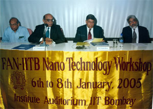
Figure 1: Dr R Chidambaram (second from left-hand side), Principal Scientific Adviser to the Govt of India (2001-18) at International Workshop on Nanotechnology jointly organised by Faculty-Alumni-Network (FAN) and IIT Bombay. Dr Chidambaram highlighted the importance of Nanotechnology research for India, specifically mentioning the initiatives by the Govt of India in setting up two Centres of Excellence for research in Nanoelectronics, with one of the centres being located at IIT Bombay. (Pic courtesy: FAN-IITB Workshop 2005)
It was at this time that Dr. R. Chidambaram, the Principal Scientific Adviser (PSA) to the Government of India (2001-2018), understood the importance of the “nanoelectronics bus” for an aspirational nation like India and how daunting a challenge it is to create a semiconductor ecosystem. To advance modern semiconductors innovation, he urgently supported the setting up of state-of-the-art nanofabrication facilities (Research Fabs) at two academic centres in the country- IISc Bangalore and IIT Bombay [6]. The idea was to develop an academic knowledge base in the electronics materials and their processing technology for the Indian industry [7]. An amount of Rs.99.80 crore was approved for the establishment of the Centre for Excellence of Nanoelectronics (CEN), one each at IIT Bombay and IISc Bangalore, in 2006 by MeitY as a 5-year project [3]. This was a tectonic shift to large, consolidated, shared, infrastructure funding in two locations. Such consolidated labs are essential platforms for complex integrated chip manufacturing process flow R&D of building nanoscale structures layer by layer. This entire process flow involves approximately 100 steps of precision chemical, plasma, thermal, and photolithographic processing – run in a tightly-controlled sequence.
A recent study by Dr. Udayan Ganguly, Dr. Sandip Lashkare, and Dr. Swaroop Ganguly from IIT Bombay showed that India has quietly come a long way in terms of the transformation of its nanoelectronics research ecosystem development [8, 9]*. Their landscape analysis highlighted that from globally negligible contributions as late as 2011, India has risen now to become globally competitive. They analysed the annual performance report of the IEEE Electron Device Letters (EDL) journal, and Transactions on Electron Devices (TED) journal. Both EDL and TED are considered the most exclusive venues to publish electron device-related research. India with 40 papers was ranked 8th in the contribution to EDL by countries, whereas the IIT System with 34 papers was ranked 9th among organizations. The IIT system was ranked 1st in the contribution to TED by organizations and India was ranked 3rd (Figure -2). Citations per paper were comparable to the journal average—slightly better than National Chiao Tung University (NCTU), Taiwan, and Chinese Academy of Science (CAS), which are similarly aged institutions, but worse than University of California System, USA (UC), which is an older player.
![Figure-2: Contributions to Electron Device Letters (EDL) journal, and Transactions on Electron Devices (TED) journal- country-wise (a,c) and organization-wise (b,d). (Pic Courtesy: IEEE EDL [7])](https://www.psa.gov.in/CMS/web/sites/default/files/inline-images/India%20rise%20picture%20insert.png)
Figure-2: Contributions to Electron Device Letters (EDL) journal, and Transactions on Electron Devices (TED) journal- country-wise (a,c) and organization-wise (b,d). (Pic Courtesy: IEEE EDL [7])
Growth in nanoelectronics engineering research from limited contributions before 2011 to high intensity by 2018 is a significant success of the strong nanoelectronics program starting in 2006 initiated together by the efforts of the Office of the PSA and MeitY. The period from initiation of the program to becoming top contributor can be divided into two phases viz. (a) six-year incubation time from infrastructure initiation to first papers, and (b) four more years to become globally competitive.
Such a successful implementation of the CEN/nanoelectronics program along with robust R&D funding and mission-mode execution should inspire a call of action for the Indian research ecosystem to contribute to the urgent national and global needs of an innovation-driven ecosystem. India must build on its success to play a significant role in this new world of disruptive innovation where Beyond Moore offers open opportunities in materials, devices to systems, and algorithms. It is possible by sustaining and amplifying successful strategies of national research infrastructure & funding growth; enhancing international collaborations to scale-up R&D infrastructure and strengthening the industry-academia-policy consortium approach to transform to an innovation-based economy.
* The original study was posted in ArXiv and an abridged version was published in IEEE Electron Device Society Newsletterin January 2021.
References:
- Statista, 2021. Value of electronic product imported into India from financial year 2011 to 2020 (in billion Indian rupees).
- Business Standard Reporter, 2014. 65 per cent of electronic items' demand met by imports: Report. Business Standard News.
- Deshpande Sarma, S. and Anand, M., 2013. Capabilities and Governance of Nanotechnology in the Developing World: Insights from India.
- Ghosh, A. and Krishnan, Y., 2014. At a long-awaited turning point. Nature Nanotechnology, 9(7), pp.491-494.
- Ministry of Electronics and Information Technology (MeitY), 2005. Annual Report 2005-06.
- Department of Science & Technology, Govt. of India, 2018. The Fabs that gave the nano-tech leap
- Kumar, A., 2014. Nanotechnology Development in India: An Overview. Research and Information System for Developing Countries.
- Ganguly, U., Lashkare, S. and Ganguly, S., 2020. India’s Rise in Nanoelectronics Research. arXiv preprint arXiv:2011.11251.
- Ganguly, U., Lashkare, S. and Ganguly, S., 2021. India’s Rise in Nanoelectronics Research. IEEE Electron Devices Society Newsletter, 28(1), pp.46-48.


